PCB EMI Shielding: 7 Smart Strategies for Success
High-frequency electronic designs face continuous risks from unwanted electromagnetic interference. Managing PCB EMI shielding is critical for ensuring electromagnetic compatibility (EMC) and […]
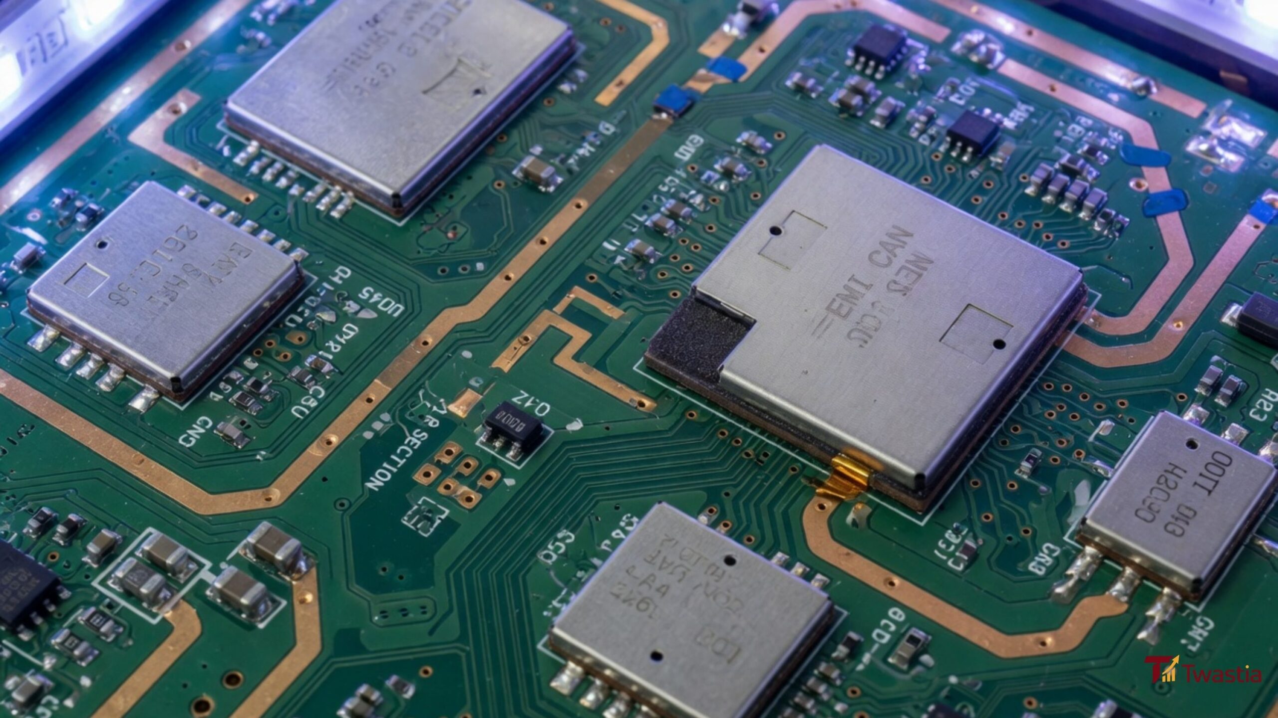
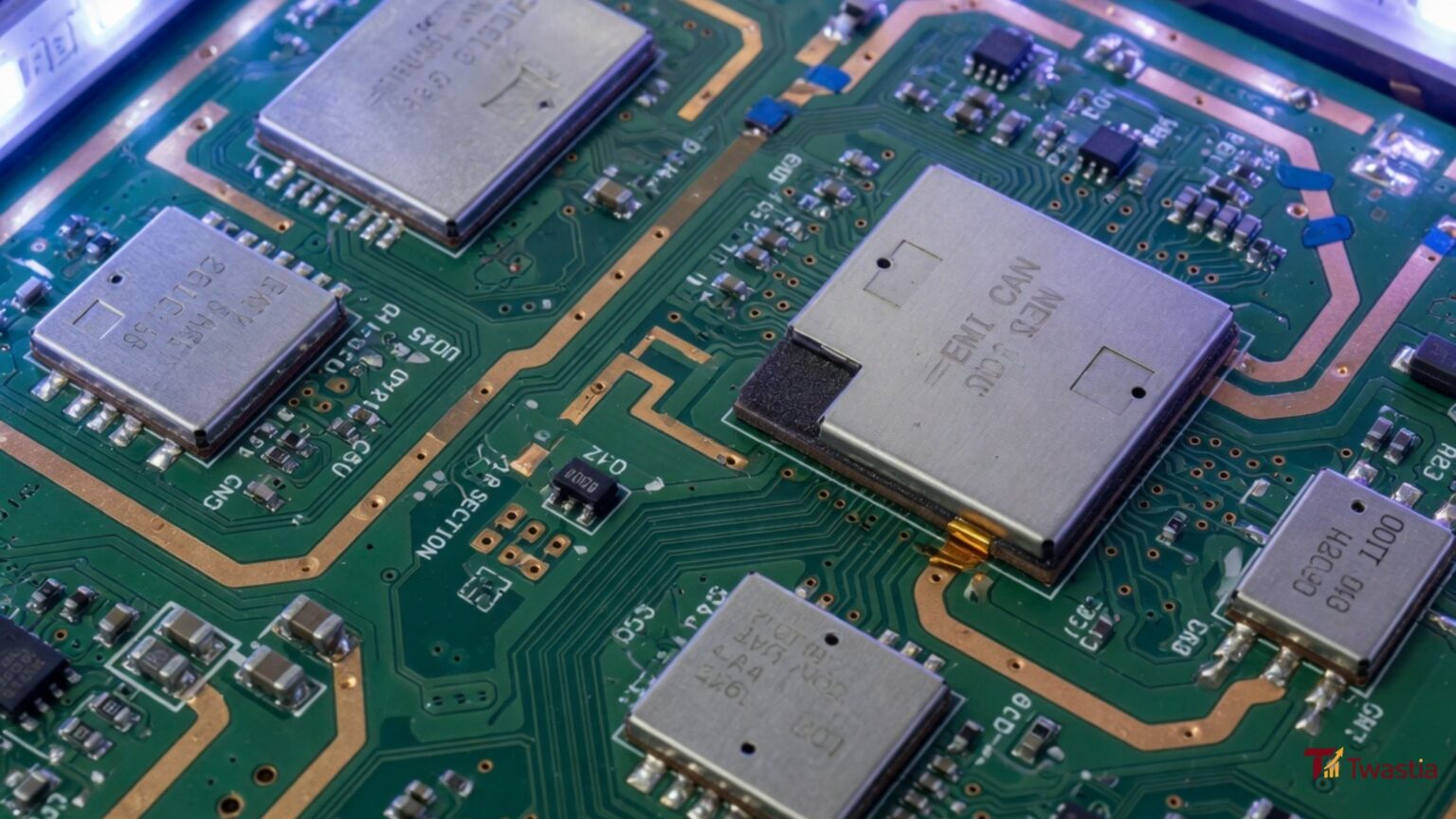
High-frequency electronic designs face continuous risks from unwanted electromagnetic interference. Managing PCB EMI shielding is critical for ensuring electromagnetic compatibility (EMC) and preventing signal degradation in modern circuit boards. As electronic components become smaller and operating clock speeds increase, trace coupling and radiated emissions become major design challenges. Unshielded electromagnetic radiation causes data corruption, timing jitter, and regulatory compliance failures during FCC or CE certification testing. Consequently, hardware engineers must integrate defensive shielding techniques throughout every stage of the printed circuit board design process. By combining board-level metallic cans, continuous ground planes, strategic component placement, and localized filtering, designers suppress electromagnetic interference effectively. This comprehensive technical guide analyzes proven shielding strategies, materials, layout rules, and compliance standards for modern high-speed circuit boards.
Understanding How PCB EMI Shielding Protects Circuits
Electromagnetic interference originates from rapid voltage changes (dV/dt) and high-speed current loops (dI/dt) across circuit board traces. Implementing a structured PCB EMI shielding approach isolates sensitive signal paths from internal and external noise sources.
| Interference Type | Physical Mechanism | Primary Shielding Defense |
|---|---|---|
| Radiated EMI | High-frequency electromagnetic waves traveling through air | Metallic board-level cans and conductive enclosures |
| Conducted EMI | Noise signals traveling directly along power and signal traces | Ferrite beads, LC filters, and decoupling capacitors |
| Capacitive Coupling | Electric field interaction between adjacent parallel traces | Interplaced ground guard traces and increased spacing |
| Inductive Coupling | Magnetic field interaction generated by signal current loops | Minimizing current loop areas and continuous ground planes |
Deploying effective board-level defenses prevents high-frequency microcontrollers, switching power supplies, and wireless transmitters from interfering with sensitive analog sensors.
7 Smart Strategies for PCB EMI Shielding Design
Achieving EMC compliance requires integrating defensive shielding principles directly into your PCB layout workflow. Below are seven proven design strategies.
1. Utilize Metallic Board-Level Shield Cans
Mounting metallic shield cans directly over sensitive circuit sections isolates high-frequency noise sources.
- Two-Piece Shield Cans: Feature a surface-mounted frame soldered to the board, accompanied by a removable snap-on lid for easy component inspection.
- One-Piece Shield Cans: Cost-effective single-cover cans soldered directly onto ground pads for permanent circuit isolation.
Consequently, placing metal cans over RF transceivers and switching regulators blocks radiated emissions before they reach nearby components.
2. Maintain Continuous Solid Ground Planes
A continuous, uninterrupted ground plane provides a low-impedance return path for high-speed signals. Avoid routing signal traces across ground plane splits, as slot gaps force return currents to travel in wide loops, creating efficient radiation antennas.
3. Implement Guard Traces and Via Fencing
Surrounding high-speed clock lines and sensitive analog traces with grounded guard traces prevents capacitive crosstalk. Furthermore, placing rows of ground vias along board edges—known as via fencing—reflects internal electromagnetic fields, preventing edge radiation.
4. Optimize Component Placement and Zoning
Group circuit components logically by operational frequency and signal type. Keep noisy digital circuits, switching power supplies, and high-frequency clock oscillators physically separated from delicate high-precision analog components.
5. Apply Conductive Coatings and Gaskets
Enclosing completed circuit assemblies inside conductive plastic housings coated with nickel, silver, or copper paint provides lightweight EMI containment. Additionally, conductive elastomer gaskets fill mechanical gaps around enclosure seams, ensuring continuous grounding.
6. Embed Traces Between Internal Ground Layers
Routing critical high-speed signal traces on internal board layers sandwiched between top and bottom ground planes creates a classic stripline structure. Consequently, the surrounding solid copper layers absorb and shield radiated fields automatically.
7. Filter Power Entry Points and High-Speed Connectors
Conducted noise enters and leaves circuit boards through external cables and power lines. Placing common-mode chokes, ferrite beads, and TVS diodes directly at board edge connectors blocks high-frequency noise before it leaks off the board.
Board-Level Shielding Material Performance Matrix
Selecting the appropriate material for metallic shield cans and enclosures dictates thermal performance, weight, and attenuation effectiveness.
| Shielding Material | Magnetic Field Shielding | Electric Field Shielding | Soldering Compatibility | Relative Material Cost |
|---|---|---|---|---|
| Nickel-Silver (NS) | Moderate | High | Excellent (Direct SMT) | Mid-Range Standard |
| Tin-Plated Steel | High (Low Frequency) | High | Excellent | Low Cost / High Weight |
| Copper-Beryllium | Moderate | Superior | Good | High-End Premium |
| Mu-Metal Alloys | Superior (Low Frequency) | Low to Moderate | Poor (Requires forming) | Specialty High-Cost |
Nickel-Silver remains the industry standard for surface-mount shield cans because it solders easily without requiring post-plating treatments.
Design Pipeline for PCB EMI Shielding Implementation
To ensure successful EMC testing, hardware teams should follow a structured layout pipeline.
| Phase 1: Floorplanning | Phase 2: Layer Stackup | Phase 3: Verification |
|---|---|---|
| Component Zoning | Ground & Shield Routing | EMC Simulation & Auditing |
| Separate analog, digital, and power sections; allocate dedicated ground pads for shield cans. | Define continuous ground reference planes, route striplines, and place edge via fencing. | Run automated 3D EM simulation software and conduct preliminary near-field scanner audits. |
Adhering to this layout pipeline minimizes redesign iterations and accelerates regulatory approval timelines.
Regulatory Standards Governing PCB EMI Shielding
Commercial electronic devices must comply with international electromagnetic compatibility regulations before entering consumer markets.
text+-----------------------------------------------------------------------------------------+
|                        INTERNATIONAL EMC REGULATORY STANDARDS                           |
+-----------------------+----------------------------------+------------------------------+
| Regulatory Agency     | Governing Standard Specification | Primary Market Compliance    |
+-----------------------+----------------------------------+------------------------------+
| FCC (USA)             | Title 47 CFR Part 15 Class B     | Consumer Electronics North US|
| CE / CISPR (Europe)   | EN 55032 / CISPR 32              | Commercial Digital Devices EU|
| ISO / CISPR (Auto)    | ISO 11452 / CISPR 25             | Automotive Electronic Modules|
| MIL-STD (Defense)     | MIL-STD-461                      | Military & Aerospace Hardware|
+-----------------------+----------------------------------+------------------------------+
Integrating robust board-level shielding ensures your designs pass FCC Class B and CE mark emissions testing on the first attempt.
Conclusion: Mastering PCB EMI Shielding Solutions
Managing electromagnetic compatibility requires a disciplined approach to circuit design, stackup selection, and mechanical containment. As detailed throughout this guide, implementing effective PCB EMI shielding protects sensitive electronics from signal degradation and costly compliance failures. By utilizing surface-mount shield cans, maintaining unbroken ground planes, routing stripline traces, and enforcing via fencing, hardware engineers suppress unwanted emissions effectively. Furthermore, filtering external cable interfaces and selecting appropriate shielding materials ensures reliable operation in high-density electronic environments. Ultimately, prioritizing board-level EMI mitigation during early layout stages accelerates product development, lowers manufacturing risks, and guarantees long-term electronic product reliability.
Frequently Asked Questions (FAQs)
What is the primary purpose of PCB EMI shielding?
It prevents internal circuits from emitting unwanted electromagnetic radiation and protects sensitive components from external electromagnetic interference.
What is the difference between a one-piece and two-piece shield can?
A one-piece can is soldered permanently over components, while a two-piece can features a soldered frame with a removable lid for easy maintenance.
Why are split ground planes dangerous for EMI design?
Routing signal traces over split ground planes forces return currents into wide loops, creating efficient antennas that radiate high-frequency noise.
How does via fencing reduce electromagnetic interference?
Via fencing uses closely spaced ground vias along board edges to create a Faraday cage effect, reflecting internal electromagnetic fields back into the board.
What shielding material is best for high-frequency RF circuits?
Nickel-Silver is ideal for RF circuits because it offers high electric field attenuation, resists corrosion, and solders directly onto PCB pads.
How close should via fencing holes be placed to suppress EMI?
Ground vias in edge fencing should be spaced no further apart than one-tenth of the highest operating frequency’s wavelength (λ/10).

Written by Twastia Editorial Team
Twastia Editorial Team shares practical insights about website design, SEO services, Google Ads, content marketing, social media, conversion rate optimization, and digital marketing strategy.
Last updated: Jul 25, 2026
Related posts from Twastia
Explore more useful articles from twastia.com about digital marketing, SEO, websites, ads, content, and growth strategy.